
Two locations, three lines
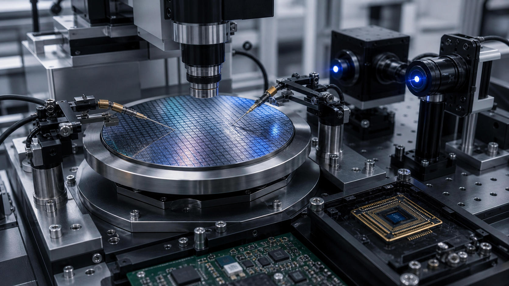
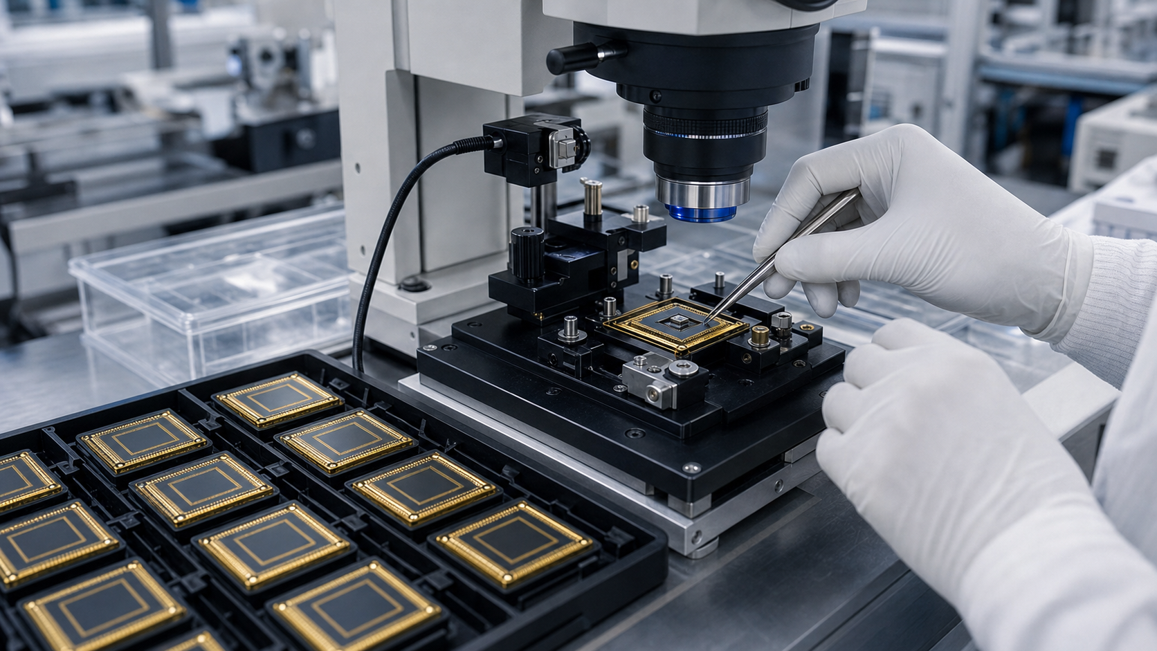
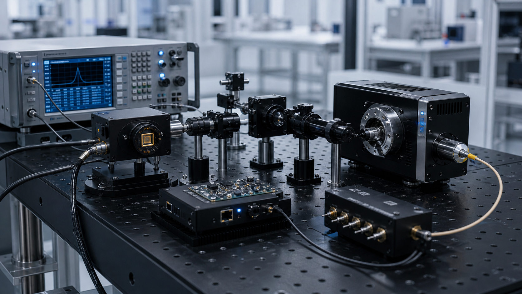
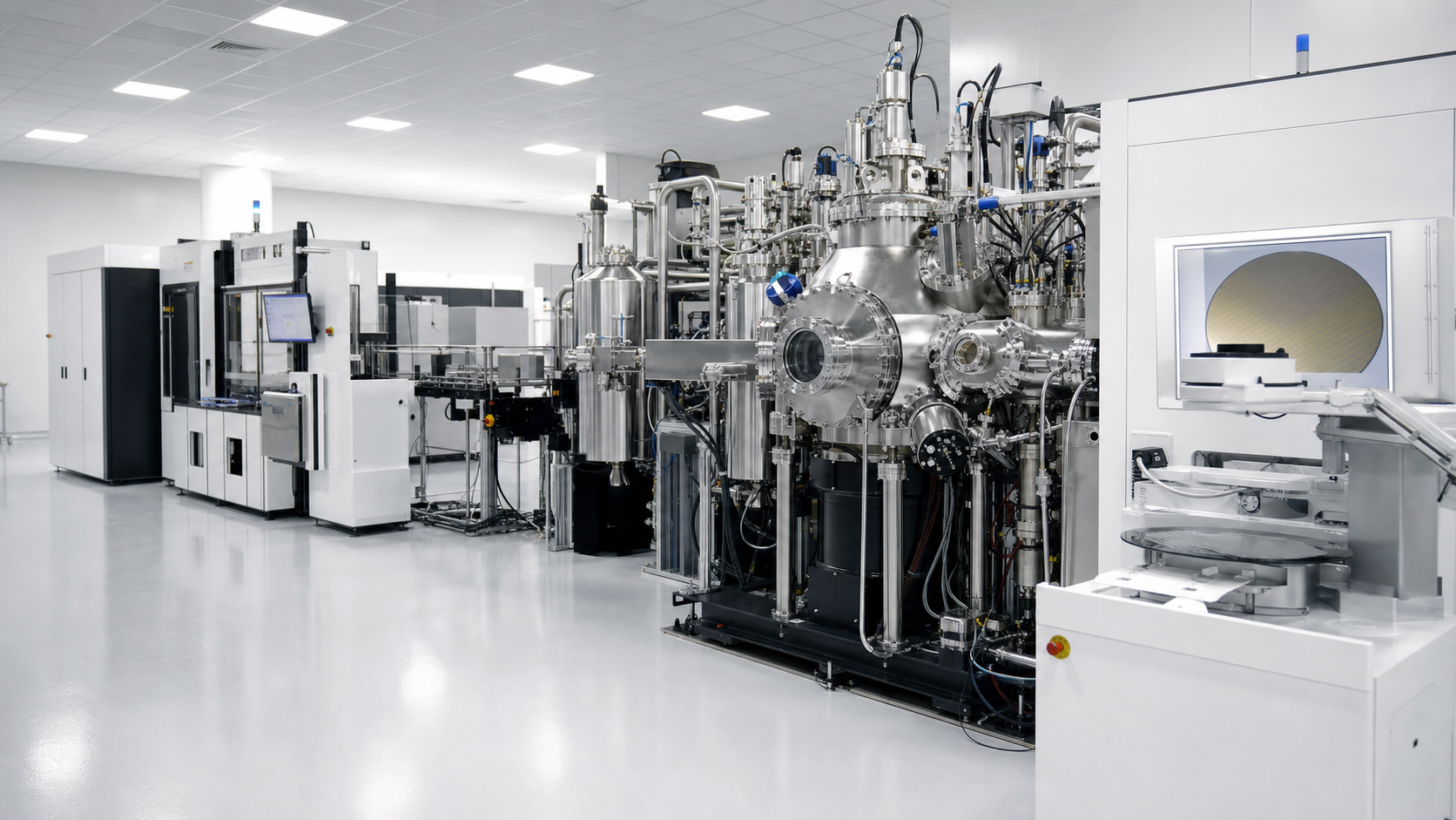
Taiyuan and Jincheng support two 4-inch lines and one 6-inch compound-semiconductor line.
Precision in chips · Intelligence in light · Vision for the future.
GK Semicoductor connects the lattice-matched 6.1 Å InAs·GaSb·AlSb material platform with epitaxy, device engineering, packaging and system integration.
Technology Platform
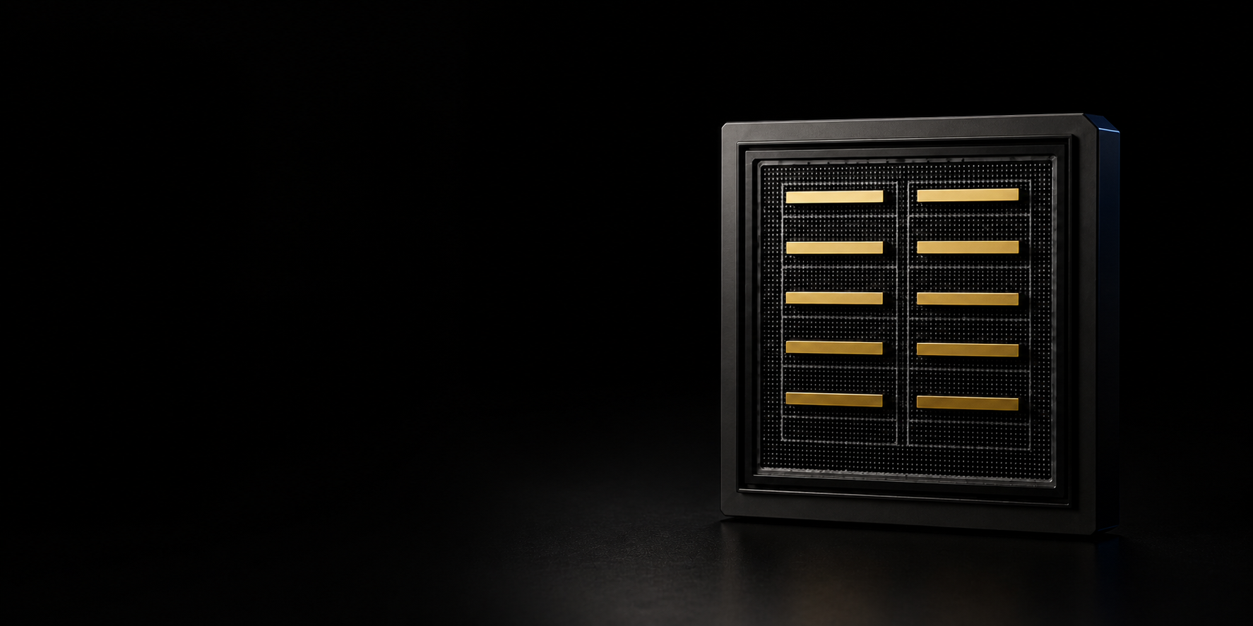
Material growth, wafer process, packaging and system integration are connected in one engineering chain.
About / Core Capabilities
Founded in 2020, GK Semicoductor is a frontier optoelectronic wafer and chip developer and manufacturer focused on III‑V compound semiconductors, particularly antimonide materials and superlattice structures.
Applications
Imaging, quantum measurement, laser processing and AI optical interconnect share one connected III-V platform.
Featured Products
A long-focal MWIR system, a megapixel cooled detector and a high-power semiconductor laser bar from the published 55-product catalog.
Manufacturing & Quality
Two locations in Taiyuan and Jincheng connect three compound-semiconductor lines with epitaxy, device engineering, packaging and system integration.
Taiyuan and Jincheng support two 4-inch lines and one 6-inch compound-semiconductor line.
Cleanroom and manufacturing space supports the documented engineering and production chain.
Material growth, device engineering, packaging and system integration are organized as one platform.
InAs, GaSb, InGaAs, InAsSb, GaAs, InP and InSb are represented in the source record.