
Route 01
Optoelectronics
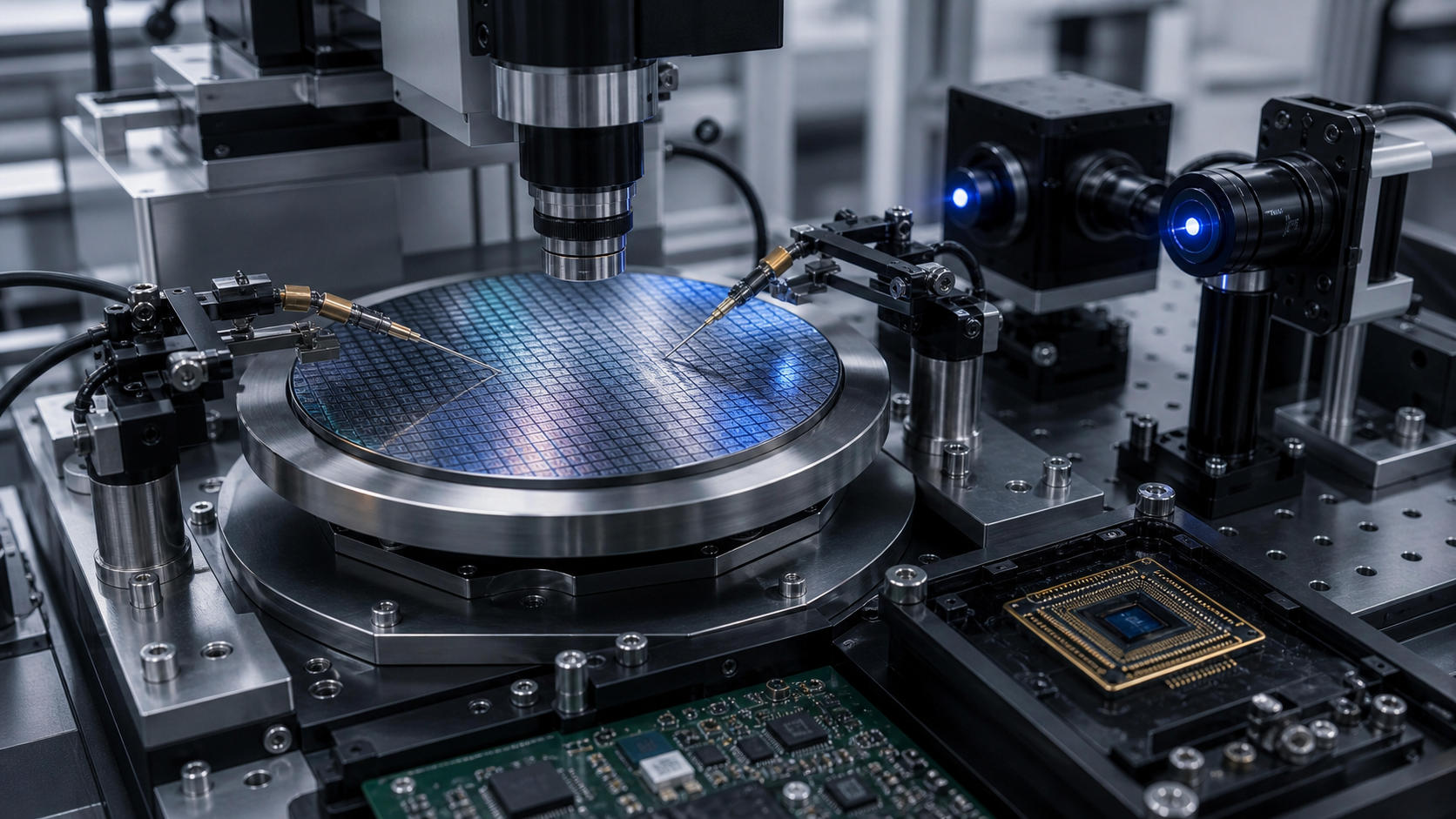
Infrared detectors, semiconductor lasers, quantum light sources and precision measurement devices.
GaSb · T2SL · QCL / ICL
III–V antimonide technology
GK Semicoductor connects the 6.1 Å InAs · GaSb · AlSb material system with epitaxy, device engineering, packaging and module integration.
01 / Platform foundation
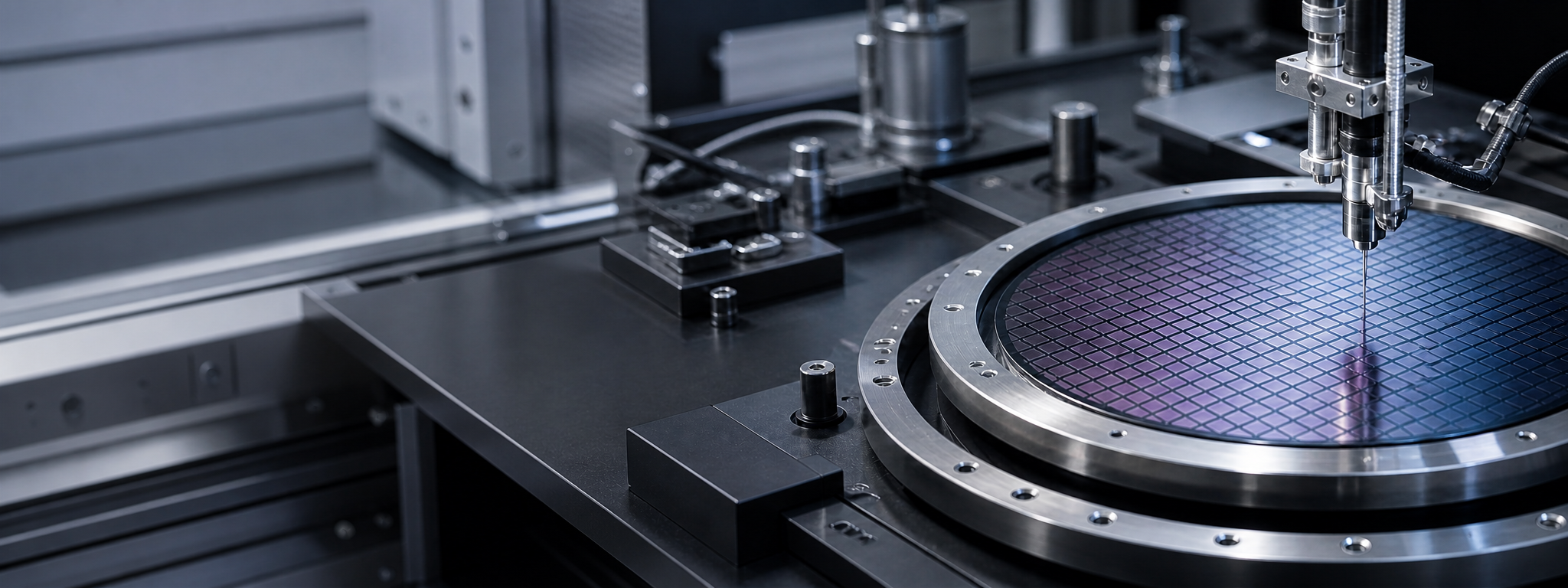
A lattice-matched 6.1 Å material foundation supports optoelectronic products today and a defined frontier route for high-speed electronics.
Infrared detectors, semiconductor lasers, quantum light sources and precision measurement devices.
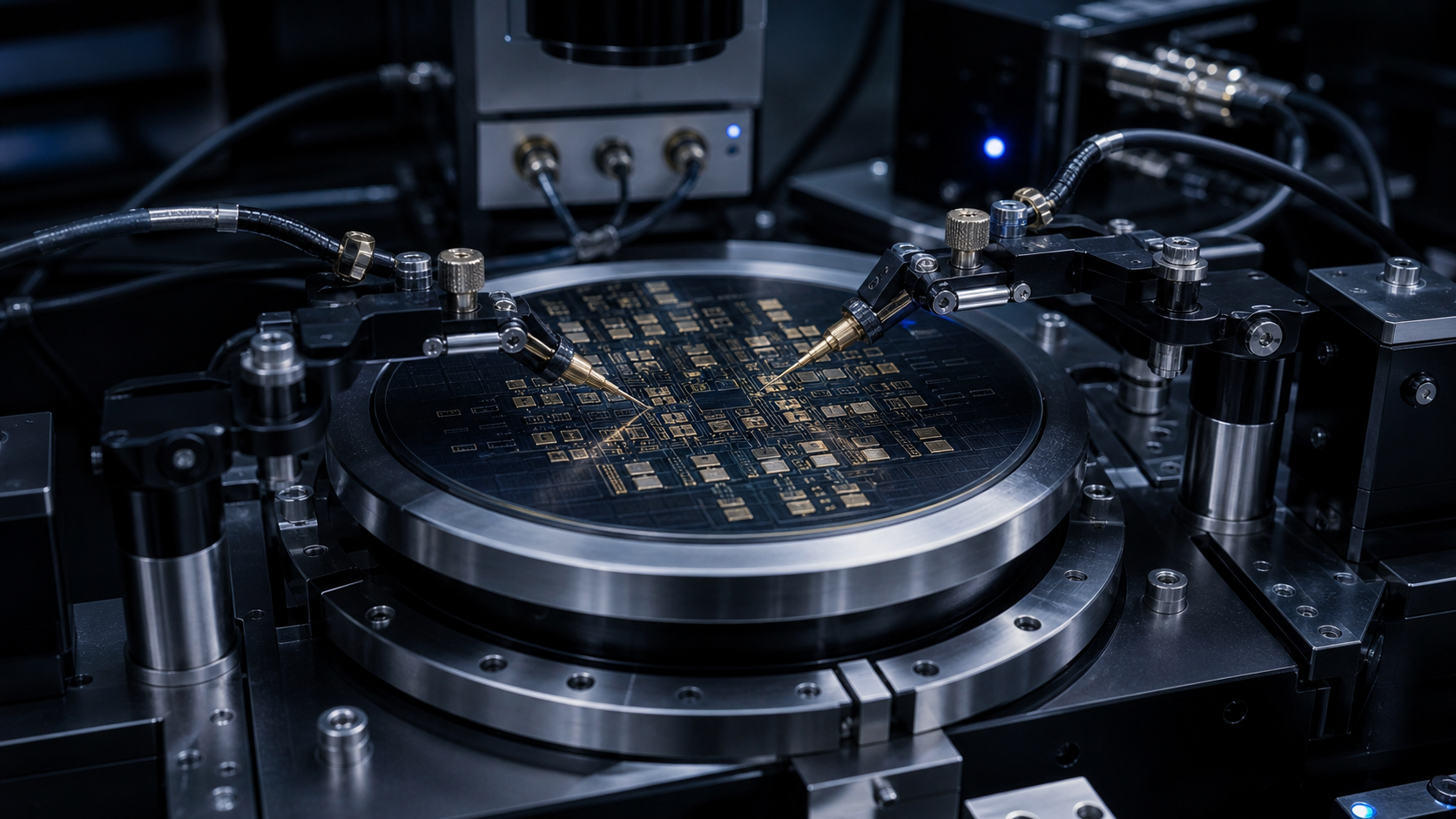
High-mobility heterojunctions for terahertz, high-frequency and low-power logic devices.
02 / Full-chain engineering
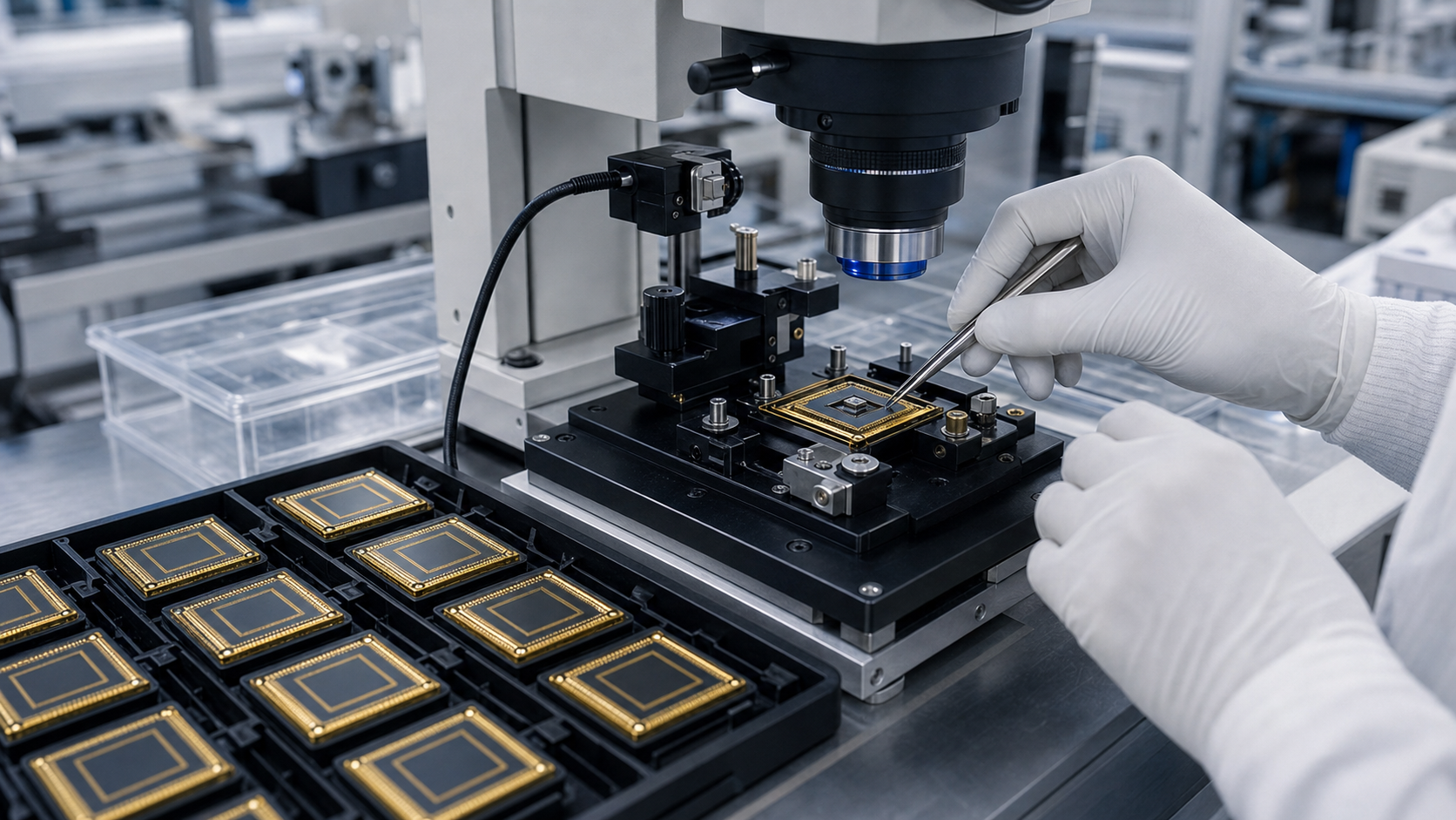
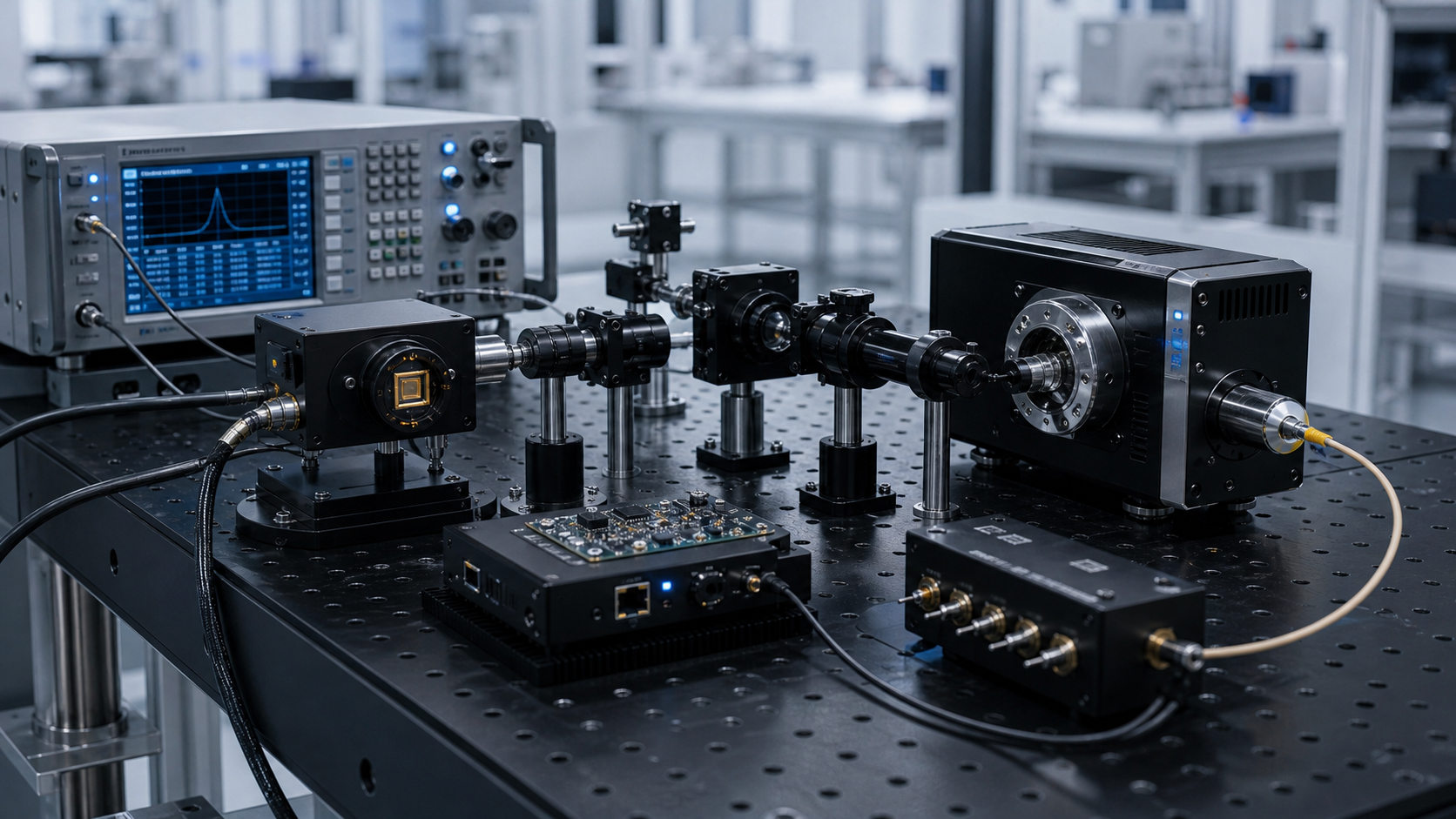
Material growth, wafer process, packaging and system integration are connected in one engineering chain.
03 / Product evidence
The source material provides device-level evidence across detector arrays and semiconductor laser products.
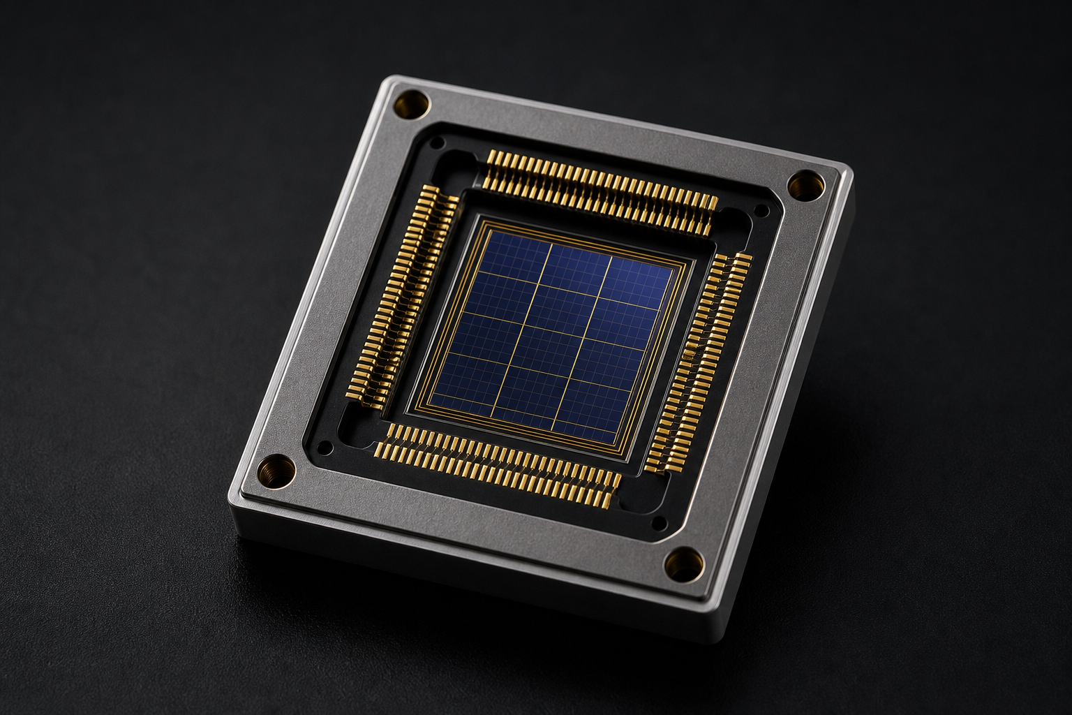
Array formats, higher operating temperature and very-long-wave response are documented in the technical record.
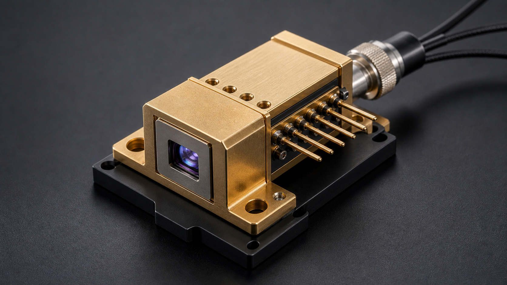
Single emitters, bars and integrated modules provide a measured path from narrow-linewidth sources to high-power output.
04 / Manufacturing and delivery
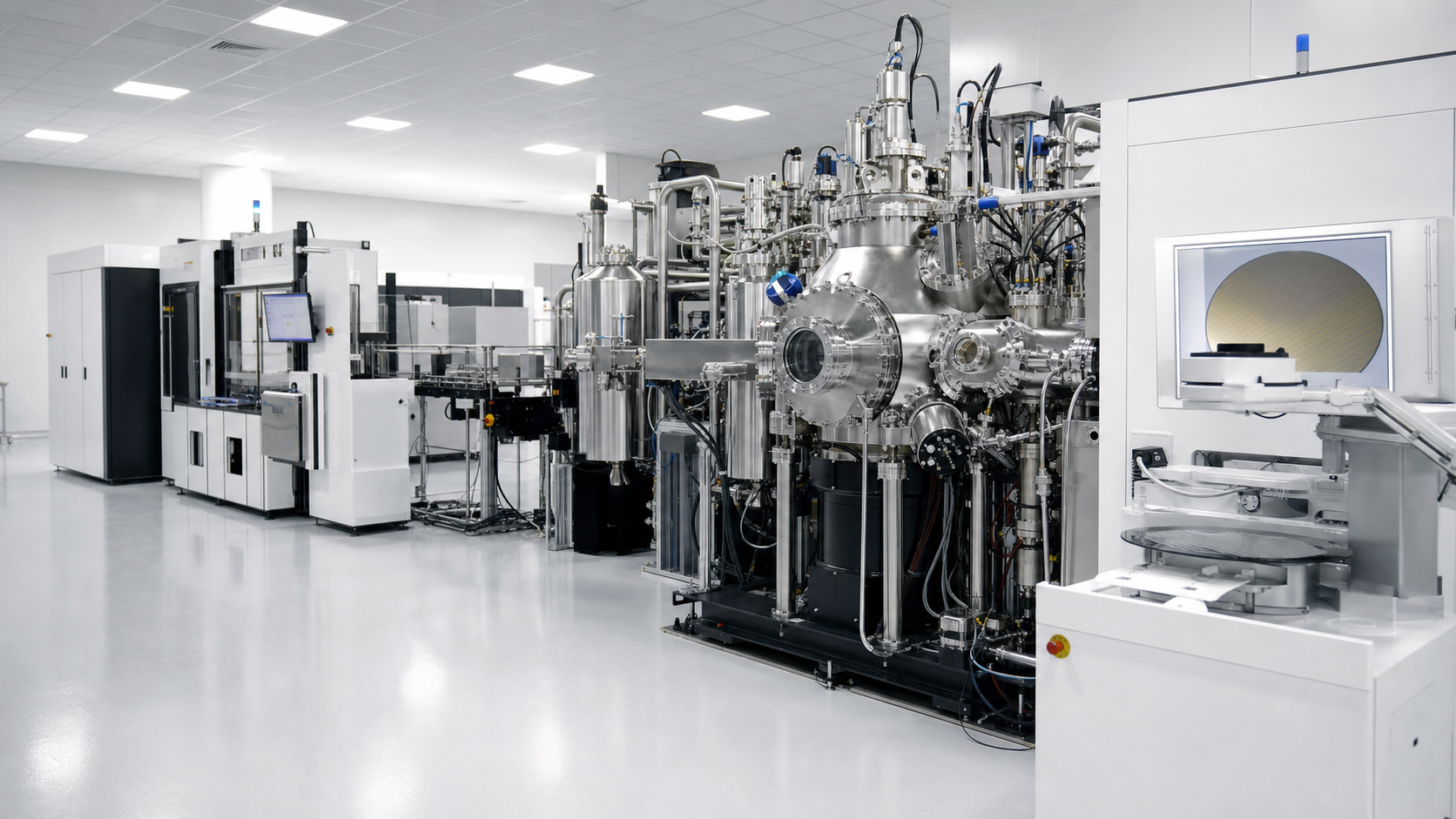
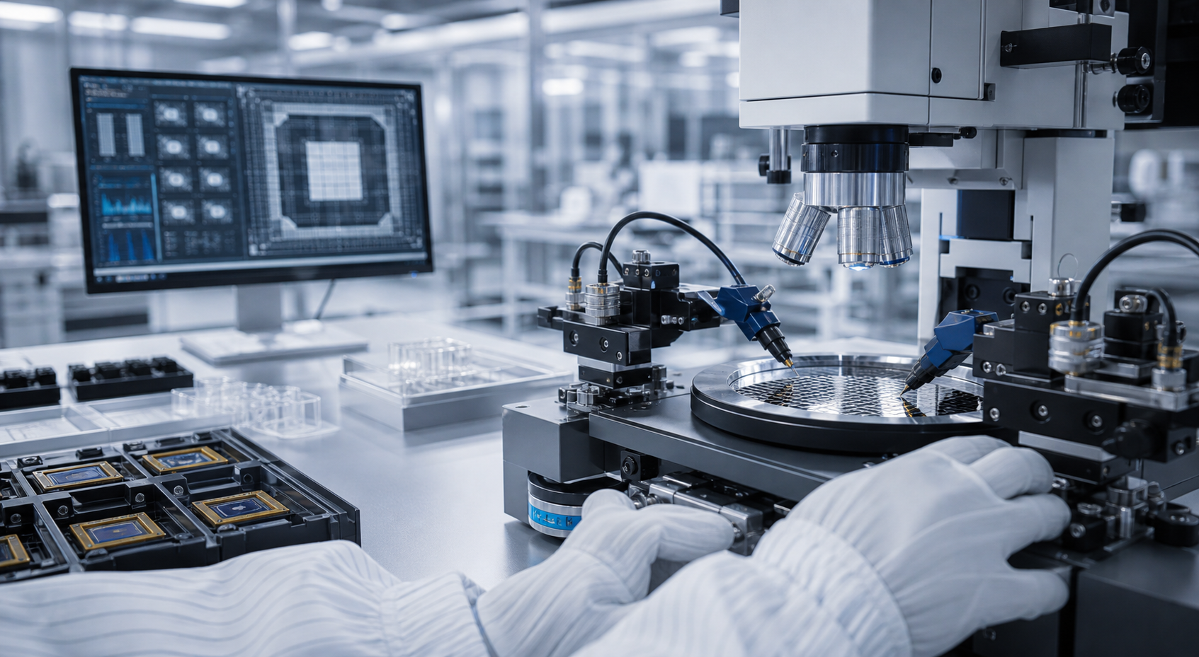
The technical record supports a connected manufacturing base across epitaxy, wafer process, packaging and module delivery.
05 / Application extensions
The current public application structure connects imaging, precision measurement, processing and optical interconnect.
GK Semicoductor connects the 6.1 Å InAs · GaSb · AlSb material system with epitaxy, device engineering, packaging and module integration.

A lattice-matched 6.1 Å material foundation supports optoelectronic products today and a defined frontier route for high-speed electronics.
Infrared detectors, semiconductor lasers, quantum light sources and precision measurement devices.
High-mobility heterojunctions for terahertz, high-frequency and low-power logic devices.
Material growth, wafer process, packaging and system integration are connected in one engineering chain.
Material design and molecular beam epitaxy establish the device foundation.
Architecture and wafer process turn material performance into device performance.
Thermal, optical and electrical interfaces are engineered around the device.
Detectors, laser sources and control electronics become application-ready modules.
The source material provides device-level evidence across detector arrays and semiconductor laser products.
Array formats, higher operating temperature and very-long-wave response are documented in the technical record.
Single emitters, bars and integrated modules provide a measured path from narrow-linewidth sources to high-power output.
The technical record supports a connected manufacturing base across epitaxy, wafer process, packaging and module delivery.
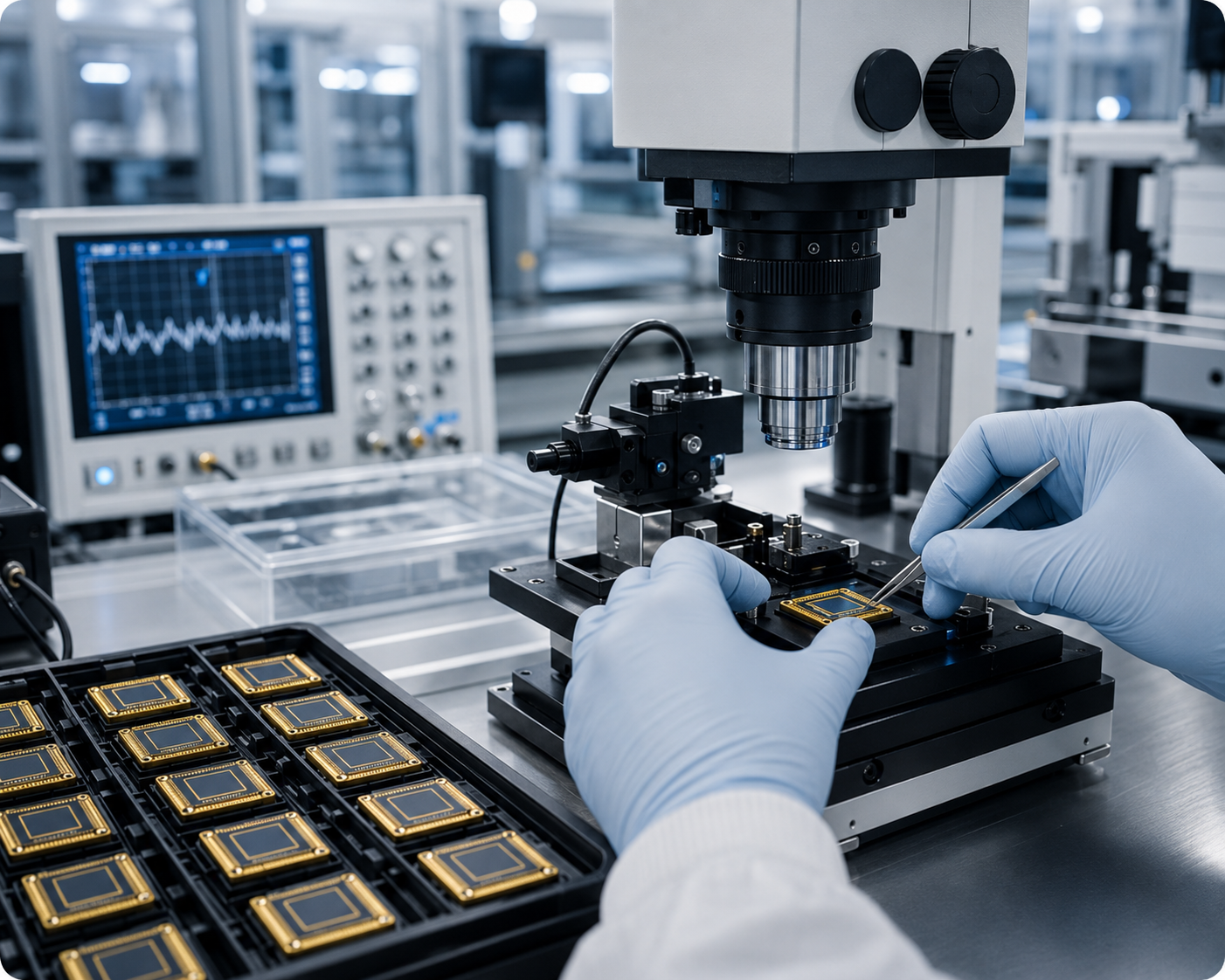
From wafer growth and chip process to package verification and system integration, the same engineering chain continues into production.
The current public application structure connects imaging, precision measurement, processing and optical interconnect.
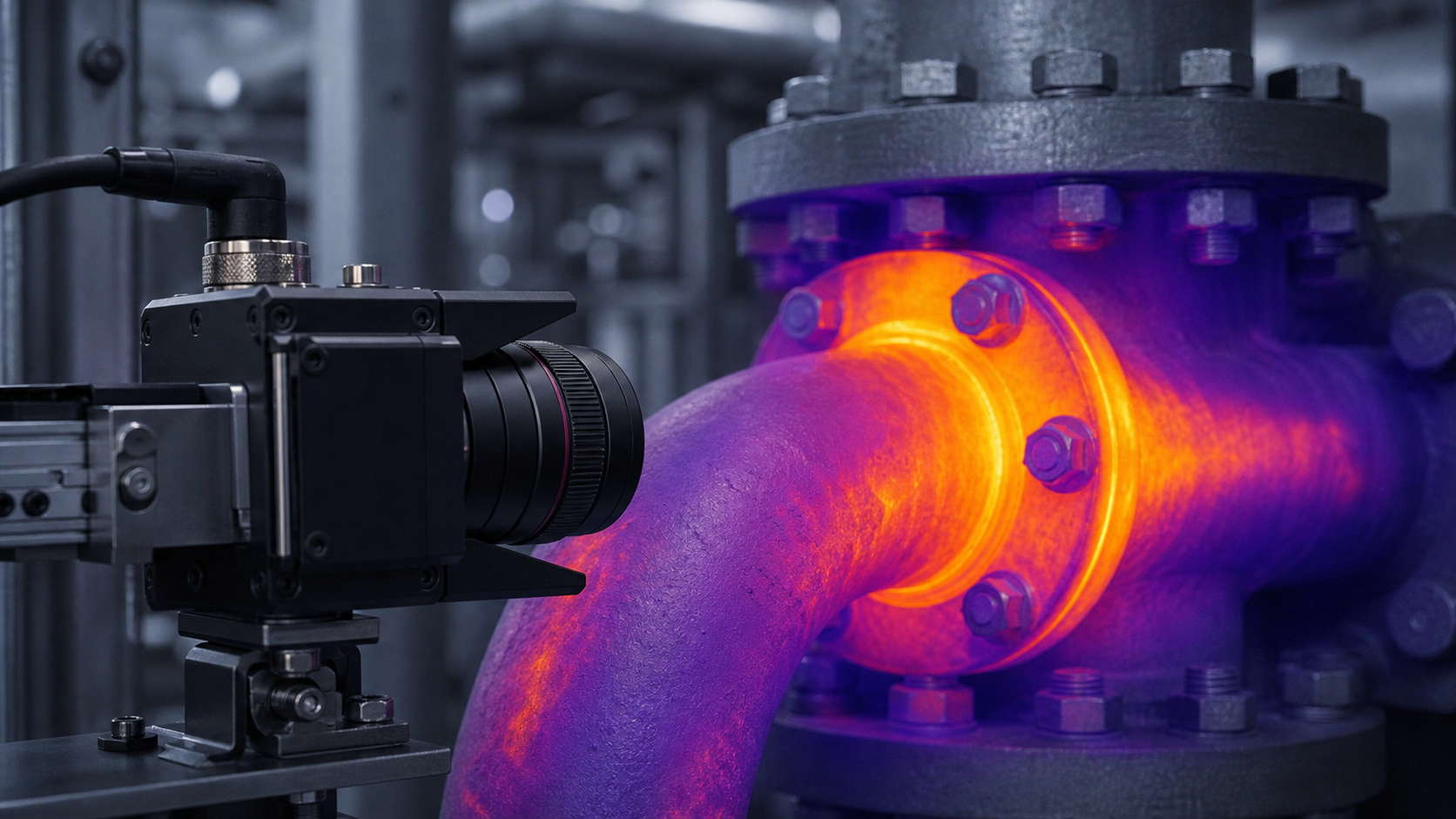 01Imaging & Ranging
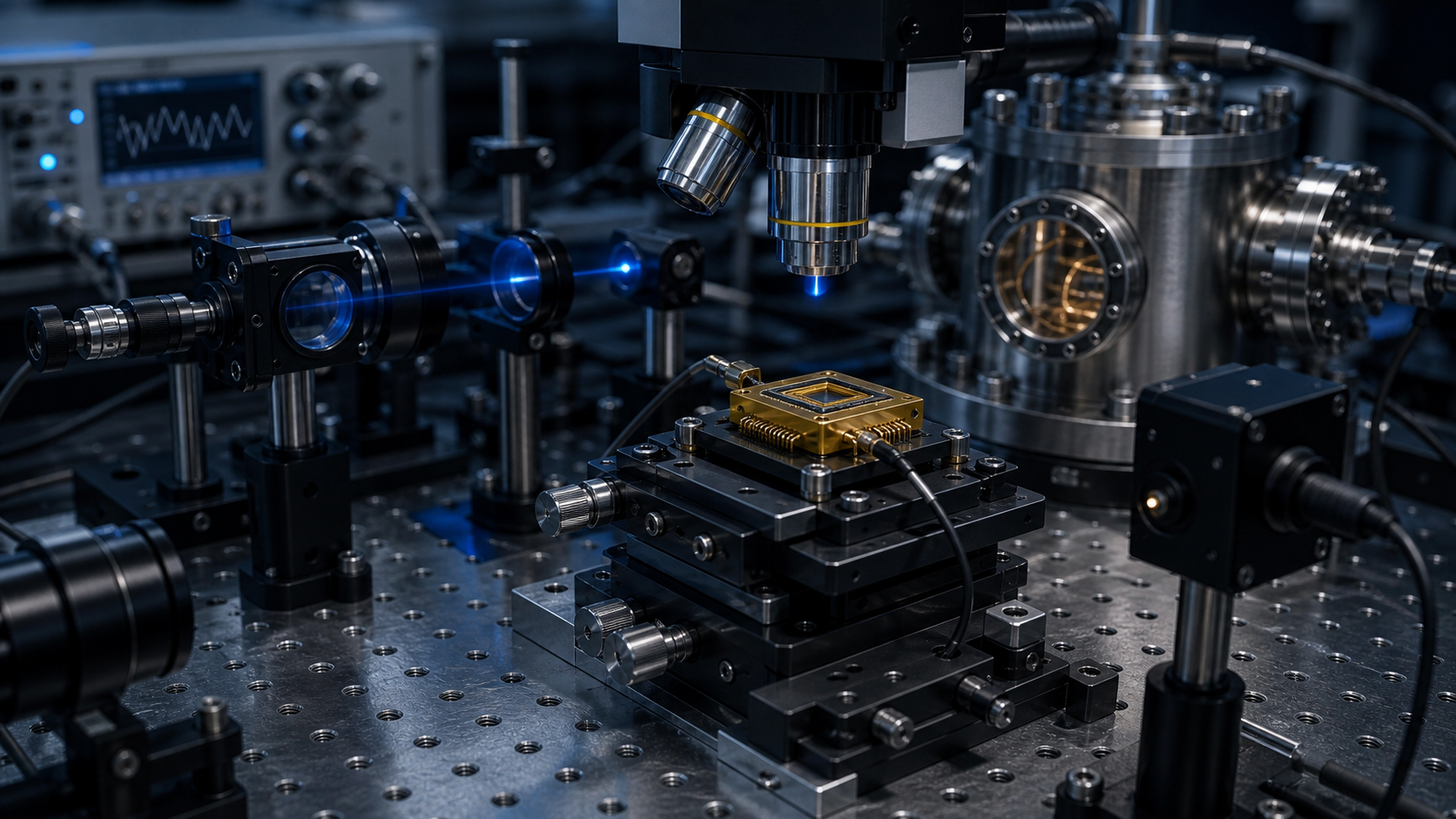 02Quantum & Precision Measurement
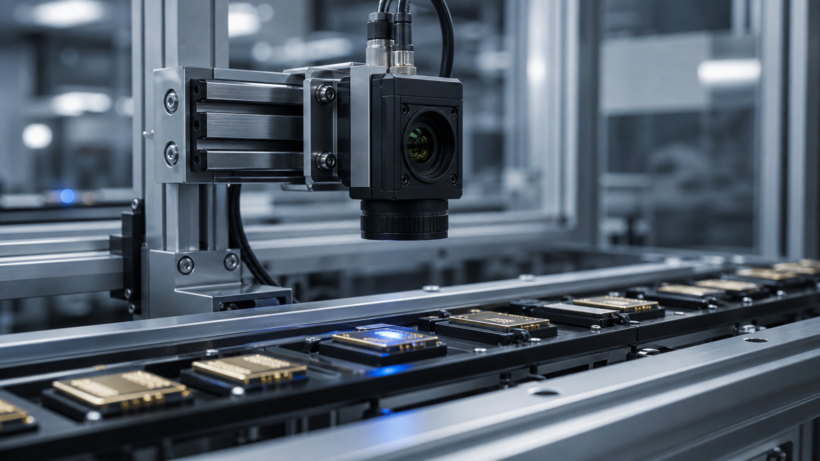 03Processing & Medical
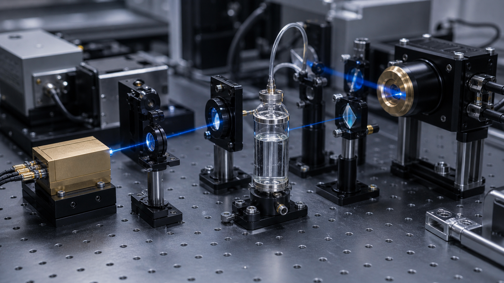 04AI Optical Interconnect